Skip to content

How to express packing that introduces constant nets #654

New issue

Have a question about this project? Sign up for a free GitHub account to open an issue and contact its maintainers and the community.

By clicking “Sign up for GitHub”, you agree to our terms of service and privacy statement. We’ll occasionally send you account related emails.

Already on GitHub? Sign in to your account

Closed
litghost opened this issue Jun 17, 2019 · 9 comments
Closed

How to express packing that introduces constant nets #654

litghost opened this issue Jun 17, 2019 · 9 comments
Labels

Comments

@litghost
Copy link
Collaborator

I'm trying to express a packing behavior that I think cannot be easily expressed using the arch xml format, but maybe I just haven't thought about it right.

The feature that I want to express is FF pass through by leveraging the FF in latch mode. So presume that the FF bank supports a latch mode, something akin to a gated D latch. Logic table:
Gated D latch logic table

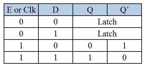
In order to treat the latch as a pass through, the CLK/gate line should be tied high, so that the latch remains passing the input to the output. However, in order for this to be true, it means that the CLK pb_type pin needs to be a specific value, e.g. high in this case. But as far as I know, there is no way to express "when using this packing, the following net must exist".

What is the recommended solution? Will this require a new feature in VPR to express such a construct?

Here is a reduced version of the pb_type for illustration:

<!-- Model of FF group in SLICEL and SLICEM -->                                   
<pb_type name="SLICE_FF" num_pb="1" xmlns:xi="http://www.w3.org/2001/XInclude">
  <!-- CK, CE and SR are slice wide. -->                                          
  <input name="CE"  num_pins="8"/>                                                
  <input name="SR"  num_pins="8"/>                                                
  <clock name="CK"  num_pins="1"/>                                                
                                                                                  
  <input  name="D"  num_pins="4"/>                                                
  <output name="Q"  num_pins="4"/>                                                
  <input  name="D5" num_pins="4"/>                                                
  <output name="Q5" num_pins="4"/>                  
                                    
  <mode name="FF_PASSTHROUGH">                                                    
    <interconnect>
      <!-- How to require that CK be connected to VCC / 1 -->
      <direct name="AFF.PASS" input="SLICE_FF.D[0]" output="SLICE_FF.Q[0]">       
        <delay_constant max="0.264e-9" in_port="SLICE_FF.D[0]" out_port="SLICE_FF.Q[0]" />                                                            
      </direct>                                                                   
      <direct name="BFF.PASS" input="SLICE_FF.D[1]" output="SLICE_FF.Q[1]">       
        <delay_constant max="0.264e-9" in_port="SLICE_FF.D[1]" out_port="SLICE_FF.Q[1]" />
      </direct>                                                                   
      <direct name="CFF.PASS" input="SLICE_FF.D[2]" output="SLICE_FF.Q[2]">       
        <delay_constant max="0.264e-9" in_port="SLICE_FF.D[2]" out_port="SLICE_FF.Q[2]" />
      </direct>                                                                   
      <direct name="DFF.PASS" input="SLICE_FF.D[3]" output="SLICE_FF.Q[3]">       
        <delay_constant max="0.264e-9" in_port="SLICE_FF.D[3]" out_port="SLICE_FF.Q[3]" />                                                       
      </direct>                                                                   
    </interconnect>                                                               
  </mode>                                                                         
  <mode name="FDSE_or_FDRE">                                                      
    <pb_type name="FF_FDSE_or_FDRE" num_pb="4">
      <input  name="D"  num_pins="1"/>                                         
      <input  name="CE" num_pins="1"/>                                                                                                                                                                             
      <clock  name="C"  num_pins="1"/>                                         
      <input  name="SR" num_pins="1"/>                                         
      <output name="Q"  num_pins="1"/>                                         
                                                                               
      <mode name="FDSE">                                                       
        <pb_type name="FDSE" num_pb="1" blif_model=".subckt FDSE_ZINI">        
          <input  name="D"  num_pins="1"/>                                     
          <input  name="CE" num_pins="1"/>                                     
          <clock  name="C"  num_pins="1"/>                                     
          <input  name="S"  num_pins="1"/>                                     
          <output name="Q"  num_pins="1"/>                                     
          <T_setup    value="{setup_CLK_DIN}"   port="D"  clock="C" />         
          <T_setup    value="{setup_CLK_CE}"    port="CE" clock="C" />         
          <T_setup    value="{recovery_CLK_SR}" port="S"  clock="C" />         
          <T_hold     value="{hold_CLK_DIN}"    port="D"  clock="C" />         
          <T_hold     value="{hold_CLK_CE}"     port="CE" clock="C" />         
          <T_hold     value="{removal_CLK_SR}"  port="S"  clock="C" />         
          <T_clock_to_Q max="{iopath_CLK_Q}"    port="Q"  clock="C" />                                                             
        </pb_type>                                                             
        <interconnect>                                                         
          <direct name="D"  input="FF_FDSE_or_FDRE.D"  output="FDSE.D" />      
          <direct name="CE" input="FF_FDSE_or_FDRE.CE" output="FDSE.CE" />
          <direct name="C"  input="FF_FDSE_or_FDRE.C"  output="FDSE.C" />      
          <direct name="S"  input="FF_FDSE_or_FDRE.SR" output="FDSE.S" />        
          <direct name="Q"  input="FDSE.Q" output="FF_FDSE_or_FDRE.Q" />       
        </interconnect>                                                        
      </mode>
      <mode name="FDRE">                                                       
        <pb_type name="FDRE" num_pb="1" blif_model=".subckt FDRE_ZINI">        
          <input  name="D"  num_pins="1"/>                                     
          <input  name="CE" num_pins="1"/>                                     
          <clock  name="C"  num_pins="1"/>                                     
          <input  name="R"  num_pins="1"/>                                     
          <output name="Q"  num_pins="1"/>                                     
          <T_setup    value="{setup_CLK_DIN}"   port="D"  clock="C" />         
          <T_setup    value="{setup_CLK_CE}"    port="CE" clock="C" />         
          <T_setup    value="{recovery_CLK_SR}" port="R"  clock="C" />         
          <T_hold     value="{hold_CLK_DIN}"    port="D"  clock="C" />         
          <T_hold     value="{hold_CLK_CE}"     port="CE" clock="C" />         
          <T_hold     value="{removal_CLK_SR}"  port="R"  clock="C" />         
          <T_clock_to_Q max="{iopath_CLK_Q}"    port="Q"  clock="C" />                                                 
        </pb_type>                                                             
        <interconnect>                                                         
          <direct name="D"  input="FF_FDSE_or_FDRE.D"  output="FDRE.D" />      
          <direct name="CE" input="FF_FDSE_or_FDRE.CE" output="FDRE.CE"/>
          <direct name="C"  input="FF_FDSE_or_FDRE.C"  output="FDRE.C" />      
          <direct name="R"  input="FF_FDSE_or_FDRE.SR" output="FDRE.R"/>                
          <direct name="Q"  input="FDRE.Q" output="FF_FDSE_or_FDRE.Q" />       
        </interconnect>                                                        
      </mode>                                                                           
    </pb_type> 
  </mode>
</pb_type>
@litghost litghost changed the title How to express packing that introduces nets How to express packing that introduces constant nets Jun 17, 2019
@litghost
Copy link
Collaborator Author

@mithro @vaughnbetz @kmurray

@litghost
Copy link
Collaborator Author

Poke @vaughnbetz @kmurray

@vaughnbetz
Copy link
Contributor

Yes, this looks like a tricky one. When you say the clk needs to be set high on the clk pb_type pin, I think you mean that the one slice-wide clock must be set to vcc for any of the latches/FFs to be used as route throughs. Is that right? That constraint could probably be modeled as a mode that put the entire slice into a mode where you can only use the latches as route-throughs, but that doesn't seem very useful or worth the complexity.

Before getting into the details of how to support that though, what is the goal / upside? Are you just trying to make FFs usable as route-throughs to gain a small amount of routability, or is there some functionality that requires this? If you're just trying to gain a small amount of routability I'd put this on the back burner, as route-throughs like this aren't nearly as important as general packing, placement and routing optimization quality. So adding complexity to try to leverage them is most likely to be counter-productive if you're just trying to obtain QoR, as it will take effort away from more important QoR tasks.

@litghost
Copy link
Collaborator Author

litghost commented Jun 20, 2019

Yes, this looks like a tricky one. When you say the clk needs to be set high on the clk pb_type pin, I think you mean that the one slice-wide clock must be set to vcc for any of the latches/FFs to be used as route throughs. Is that right? That constraint could probably be modeled as a mode that put the entire slice into a mode where you can only use the latches as route-throughs, but that doesn't seem very useful or worth the complexity.

I completely agree with this sentiment, however!

So adding complexity to try to leverage them is most likely to be counter-productive if you're just trying to obtain QoR, as it will take effort away from more important QoR tasks.

A QoR change in Yosys (e.g. synthesis change) is what brought this about. In particular, the CARRY4 primitive has 8 outputs (4 CO and 4 O). If those outputs are not registered (e.g. no FF directly at the output), then 8 ports are required. By default only 4 ports are available, unless the FF's are put into passthrough.

That constraint could probably be modeled as a mode that put the entire slice into a mode where you can only use the latches as route-throughs, but that doesn't seem very useful or worth the complexity.

Your understanding is exactly correct, and exactly what Vivado does if more than 4 ports from a CARRY4 is required.

@litghost
Copy link
Collaborator Author

I think in the short term, I'll see if I can make Yosys return a synthesis that doesn't require this feature, and we can delay support of it.

@vaughnbetz
Copy link
Contributor

Sounds good. If you want to flip the whole mode it's probably doable with an architecture file change.

But it is quite rare for a design to need both the CO and O (sumout?) signals, except that the next bit of the carry chain needs the CO output, but that should be done with dedicated routing.
Altera/Intel devices don't even allow you to get the CO signal out to general routing; if you want the top CO bit you add one bit to the carry chain and it comes out as a sumout. So if there's no good reason to be sending both CO and O (sumout?) to the general routing, I'd just skip supporting it as it will probably rarely (never?) be used.

@litghost
Copy link
Collaborator Author

So if there's no good reason to be sending both CO and O (sumout?) to the general routing, I'd just skip supporting it as it will probably rarely (never?) be used.

This is the approach I'm taking. I can simply remove the CO output from the CARRY4 altogether, because as you said, you can always use the sumout as a CO.

Copy link

This issue has been inactive for a year and has been marked as stale. It will be closed in 15 days if it continues to be stale. If you believe this is still an issue, please add a comment.

@github-actions github-actions bot added the Stale label Apr 30, 2025
Copy link

This issue has been marked stale for 15 days and has been automatically closed.

@github-actions github-actions bot closed this as not planned Won't fix, can't repro, duplicate, stale May 16, 2025
Sign up for free to join this conversation on GitHub. Already have an account? Sign in to comment
Labels
Projects
None yet
Development

No branches or pull requests

2 participants